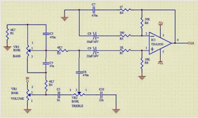
Period To Voltage Converter Circuit Diagram
The input signal drives ICD. Because ICD`s positive input (V+) is slightly offset to + 0.1 V, its steady stateoutput will be around +13 V. This voltage is sent to ICC through D2, setting ICC`s output to +13 V. Therefore, point D is cut off by Dl, and CI is charged by the current source. Assuming the initial voltage on CI is zero, the maximum voltage (^Cinax) is given by:
This is a simple Period-To-Voltage Converter Circuit Diagram. When the input goes from low to high, a narrow positive pulse is generated at point A. This pulse becomes -13 V at point B, which cuts off D2. ICC`s V+ voltage becomes zero. The charge on CI will be absorbed by ICC on in a short time.
The time constant of C2 and R5 determines the discharge period— about 10 /is. ICB is a buffer whose gain is equal to (R& + R9)~Rg = lM5. ICD`s average voltage will be (1362f 1.545) + 2 = 1052/. RIO and C3 smooth the sawtooth waveform to a dc output.
Period-To-Voltage Converter Circuit Diagram

Build a Period-To-Voltage Converter Circuit Diagram


Comments
Post a Comment