Posts

Showing posts with the label Converter

1 5V Battery to 5V Voltage Converter Circuit Diagram
Image
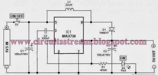
This is a Simple 1.5V Battery to 5V Voltage Converter Circuit Diagram. Stable and secure 5V DC (at 200mA max) from an ordinary 1.5V AA sized cell. At the heart of this circuit is IC1 MAX756 from Maxim, which is a CMOS step-up DC-DC switching regulator for small, low input voltage or battery-powered systems.   Simple 1.5V Battery to 5V Voltage Converter Circuit Diagram MAX756 accepts a positive input voltage down to 0.7V and converts it to a higher pin selectable output voltage of 5V (or 3.3V). Typical full-load efficiency for the this IC is greater than 87%. Max756 combine a switch-mode regulator with an N-channel MOSFET, precision voltage reference, and power-fail detector in a single monolithic device. The MOSFET is a “sense-FET” type for best efficiency, and has a very low gate threshold voltage to ensure start-up under low-battery voltage conditions (1.1V typ). The circuit can be easily wired on a very small rectangular common PCB.All connections should be kept as short as poss...

3V to 40 Volt DC Converter Circuit

Image
Switching regulator subsystems intended for use asdc to dc converters. 3V to 40 Volt DC Converter circuit | The use of switching regulators is becoming more pronounced over that of linear regulators because the size reductions in new equipment designs require greater conversion efficiency. Another major advantage of the switching regulator is that it has increasednapplication flexibility of output voltage. The output can be less than, greater than, or of opposite polarity to that of the input voltage. The MC34063 series is a monolithic control circuit containing all the active functions required for dc to dcconverters. This device contains an internal temperature compensated reference, comparator, controlled duty cycle oscillator with an active peak current limit circuit, driver, and a high current output switch. This series was specifically designed to be incorporated in step–up, step–down and voltage– inverting converter a...

Simple Sine Wave To Square Wave Converter Circuit Diagram

Image
This is the Simple Sine Wave To Square Wave Converter Circuit Diagram. This circuit turns a sine wave into a square wave. It is comprised of a single 2-input NAND Schmitt trigger that`s configured as an inverter with a trigger level adjustment at its input. As the input voltage rises above the gate`s trigger point, the output snaps to its alternate state, producing a square-wave output. Simple Sine Wave To Square Wave Converter Circuit Diagram

Step Up Converter For 20 LEDs

Image
The circuit described here is a step-up converter to drive 20 LEDs, designed to be used as a home-made ceiling night light for a child’s bedroom. This kind of night light generally consists of a chain of Christmas tree lights with 20 bulbs each consuming 1 W, for a total power of 20 W. Here, in the interests of saving power and extending operating life, we update the idea with this simple circuit using LEDs.  Power can be obtained from an unregulated 12 V mains adaptor, as long as it can deliver at least about 330 mA.  The circuit uses a low-cost current-mode controller type UCC3800N, reconfigured into voltage mode to create a step-up converter with simple compensation. By changing the external components the circuit can easily be modified for other applications. To use a current-mode controller as a voltage-mode controller it is necessary to couple a sawtooth ramp (rising from 0 V to 0.9 V) to the CS (current sense) pin, since this pin is also an input to the internal PWM com...

Period To Voltage Converter Circuit Diagram

Image
The input signal drives ICD. Because ICD`s positive input (V+) is slightly offset to + 0.1 V, its steady stateoutput will be around +13 V. This voltage is sent to ICC through D2, setting ICC`s output to +13 V. Therefore, point D is cut off by Dl, and CI is charged by the current source. Assuming the initial voltage on CI is zero, the maximum voltage (^Cinax) is given by:  This is a simple Period-To-Voltage Converter Circuit Diagram. When the input goes from low to high, a narrow positive pulse is generated at point A. This pulse becomes -13 V at point B, which cuts off D2. ICC`s V+ voltage becomes zero. The charge on CI will be absorbed by ICC on in a short time.  The time constant of C2 and R5 determines the discharge period— about 10 /is. ICB is a buffer whose gain is equal to (R& + R9)~Rg = lM5. ICD`s average voltage will be (1362f 1.545) + 2 = 1052/. RIO and C3 smooth the sawtooth waveform to a dc output. Period-To-Voltage Converter Circuit Diagram Build a Period-To...

Valve Sound Converter Circuit Diagram

Image
‘Valve sound’ is not just an anachronism: there are those who remain ardent lovers of the quality of sound produced by a valve amplifier. However, not everyone is inclined to splash out on an expensive valve output stage or complete amplifier with a comparatively low power output. Also, for all their aesthetic qualities, modern valve amplifiers burn up (in the full sense of the word!) quite a few watts even at normal listening volume, and so are not exactly environmentally harmless. This valve sound converter offers a cunning way out of this dilemma. It is a low cost unit that can be easily slipped into the audio chain at a suitable point and it only consumes a modest amount of energy.  Valve Sound Converter Circuit Diagram A valve sound converter can be constructed using a common-or-garden small-signal amplifier using a readily-available triode. Compared to using a pentode, this simplifies the circuit and, thanks to its less linear characteristic, offers even more valve sound. Fo...

Valve Sound Converter

Image
‘Valve sound’ is not just an anachronism: there are those who remain ardent lovers of the quality of sound produced by a valve amplifier. However, not everyone is inclined to splash out on an expensive valve output stage or complete amplifier with a comparatively low power output. Also, for all their aesthetic qualities, modern valve amplifiers burn up (in the full sense of the word!) quite a few watts even at normal listening volume, and so are not exactly environmentally harmless. This valve sound converter offers a cunning way out of this dilemma. It is a low cost unit that can be easily slipped into the audio chain at a suitable point and it only consumes a modest amount of energy. . Valve Sound Converter Circuit Diagram A valve sound converter can be constructed using a common-or-garden small-signal amplifier using a readily-available triode. Compared to using a pentode, this simplifies the circuit and, thanks to its less linear characteristic, offers even more valve sound. For ...

Converter

Image

Temperature To Pulse Width Converter Using LM3524

Image
How to make a temperature to pulse width converter circuit. this is a simple circuit of temperature to pulse width converter.  The LM3524 to convert the output of an LM135 temperature transducer into a pulse width which can be measured by a digital system, such as a microprocessor controlled data acquisition system. In this circuit, the LM135’s temperature-dependent output (10 mV/°K) is divided down and applied to A1’s positive input. Temperature To Pulse Width Converter Circuit Diagram: This moves A1’s output high, driving the input to the LM3524’s pulse width modulation circuitry. The LM3524 pulse-width output is clipped by the LM185 reference and integrated by the 1 MW-0.1 µF combination. The DC level across the 0.1 µF capacitor is fed back to A1’s negative input. This feedback path forces the LM3524’s output pulse width to vary in a highly linear fashion according to the potential at A1’s positive input. Here is a schematic drawing: The overall temperature to pulse width scale ...

SW Converter for AM Radio Circuit Diagram

Image
SW Converter for AM Radio Circuit diagram. Apart from chucking it in the bin, what can you do with old AM car radio or clock radio in your junkbox? How about turning it into a crystal controlled, stable, short wave radio receiver, for a minimum investment in time and money? Read on. The heart of the circuit shown here is an IC which goes by the name NE602, NE612 or SA612. It is a double balanced mixer that includes an oscillator that can be crystal-controlled, free running or even driven externally from a PLL, etc. It was originally designed for mobile telephones and is probably available in junked car phones from the tip. The NE602/612 contains a differential input amplifier (called a Gilbert Cell), an oscillator/buffer, a temperature compensated bias network and a power regulator. Typical frequency response is in excess of 500 MHz for the input and 100 MHz for the oscillator. SW Converter for AM Radio Circuit diagram : SW Converter for AM Radio Circuit Diagram   Supply current ...

Simple 6V to 12V Converter Circuit Diagram

Image
 This inverter circuit can provide up to 800mA of 12V power from a 6V supply. For example, you could run 12V car accessories in a 6V (British?) car. The circuit is simple, about 75% efficient and quite useful. By changing just a few components, you can also modify it for different voltages. Notes L1 is a custom inductor wound with about 80 turns of 0.5mm magnet wire around a toroidal core with a 40mm outside diameter. Different values of D3 can be used to get different output voltages from about 0.6V to around 30V. Note that at higher voltages the circuit might not perform as well and may not produce as much current. You may also need to use a larger C3 for higher voltages and/or higher currents. You can use a larger value for C3 to provide better filtering. The circuit will require about 2A from the 6V supply to provide the full 800mA at 12V. 6V to 12V Converter Circuit Diagram Parts R1, R4 2 2.2K 1/4W Resistor R2, R3 2 4.7K 1/4W Resistor R5 1 1K 1/4W Resistor R6 1 1.5K 1/4W Resis...

Voltage to Frequency Converter Circuits Diagram

Image
This Simple Voltage to Frequency Converter Circuits Diagram has a 1 Hz-to-30 MHz output, 150-dB dynamic range, for a 0 to 5 V input. It maintains 0.08% linearity over its entire 71/3 decade range with a full-scale drift of about 20 ppm/°C. To get the additional bandwidth, the fast )FET buffer drives the Schottky TTL Schmitt trigger.  Simple Voltage to Frequency Converter Circuits Diagram The Schottky diode prevents the Schmitt trigger from ever seeing negative voltage at its input. The Schmitt`s input voltage hysteresis provides the limits which the oscillator runs between. The 30-MHz, full-scale output is much faster than the LTC1043 can accept, so the digital divider stages are used to reduce the feedback frequency signal by a factor of 20. The remaining Schmitt sections furnish complementary outputs.

Converter RS232 to Arduino Circuit Diagram

Image
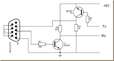
The circuit in this article is an RS232 converter , it is possible to connect an Arduino bootloader or your chip with a RS232 port . Here are two versions, one very simple and functional above and one below a little more sophisticated . The port 232 gives a bit more work than USB , but in case of equipment that only have this feature that is a good outlet .  Converter RS232 to Arduino Circuit Diagram

Voltage Converter Circuit Diagram

Image
Teledyne Semiconductor`s Type TSC9402 is a versatile IC. Not only can it convert voltage into frequency, but also frequency into voltage. It is thus eminently suitable for use in an add-on unit for measuring frequencies with a multimeter. Only a few additional components are required for this.. Just one calibration point sets the center of the measuring range (or of that part of the range that is used most frequently).  The frequency-proportional direct voltage at the output (pin 12—amp out) contains interference pulses at levels up to 0.7 V. If these have an adverse effect on the multimeter, they can be suppressed with the aid of a simple RC network.  The output voltage, U0, is calculated by: tfo=C/rei(Ci + 12 pF) R2fm Because the internal capacitance often has a greater value than the 12 pF taken here, the formula does not yield an absolute value. The circuit has a frequency range of dc to 10 kHz. At 10 kHz, the formula gives a value of 3.4 V. The circuit draws a current o...

6V to 12V Converter Circuit Diagram

Image
This inverter circuit can provide up to 800mA of 12V power from a 6V supply. For example, you could run 12V car accessories in a 6V (British?) car. The circuit is simple, about 75% efficient and quite useful. By changing just a few components, you can also modify it for different voltages. Read : 250 to 5000 watts PWM DC/AC 220V Power Inverter Notes L1 is a custom inductor wound with about 80 turns of 0.5mm magnet wire around a toroidal core with a 40mm outside diameter. Different values of D3 can be used to get different output voltages from about 0.6V to around 30V. Note that at higher voltages the circuit might not perform as well and may not produce as much current. You may also need to use a larger C3 for higher voltages and/or higher currents. You can use a larger value for C3 to provide better filtering. The circuit will require about 2A from the 6V supply to provide the full 800mA at 12V. 6V to 12V Converter Circuit Diagram Parts R1, R4 2 2.2K 1/4W Resistor R2, R3 2 4.7K 1/4W R...

Versatile DC DC Converter

Image
Here is a versatile power coupler that connects a device to 5V-19V DC generated from AC mains by a power adaptor. Power adaptors come in different voltage outputs like 5V (for mobile phones), 12V (for external hard drives) and 19V (for laptops). Sometimes the power adaptor may have a voltage rating higher than the required voltage. With the converter circuit given here, the adaptor can be used to power any device at a lower voltage.  For instance, by using a 19V laptop adaptor, you can power a TTL circuit at 5V. There can also be other instances when one needs a 3V or 6V supply. All these and many other intermediate voltages are easily possible with this versatile converter circuit when used together with any off-hand power adaptor. Versatile DC-DC Converter Circuit diagram Fig. 1 shows the circuit of the DC-DC converter. Smooth reduction in the voltage is achieved using the LM317 regulator IC. The complete unit can fit inside a piece of a glue stick tube. Adjusting variable resis...