Posts

Showing posts with the label Supply

Dual Power Supply Circuits
Image
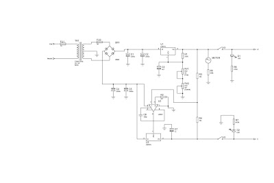
This is a bench top power supply that can be used to power circuits or devices during development work in the lab. More specifically it is an adjustable, tracking, dual rail supply which means there are two supply voltages, one positive, one negative, that are adjusted by a common potentiometer such that supply voltages are equal in magnitude. It is capable of supplying up to +/- 15V DC at up to 1A. This is sufficient for the majority of small signal electronic projects. Dual Power Suplly Circuit diagram. Click to view larger Power Supply circuit above shows the circuit layout for this project. A centre tapped transformer (TR1) is used with two 12V secondary windings with its centre tap tied to ground. This allows positive and negative voltages to be generated with respect to the central ground. Rectification follows based upon the bridge rectifier (BR1) and smoothing capacitors (C1, C2, C4 and C5). Two linear regulators are used, an LM317 on the positive side and an LM337 on the ne...

Mains Supply Failure Alarm

Image
Whenever AC mains supply fails, this circuit alerts you by sounding an alarm. It also provides a backup light to help you find your way to the torch or the generator key in the dark. The circuit is powered directly by a 9V PP3/6F22 compact battery. Pressing of switch S1 provides the 9V power supply to the circuit. A red LED (LED2), in conjunction with zener diode ZD1 (6V), is used to indicate the battery power level. Resistor R9 limits the operating current (and hence the brightness) of LED2. When the battery voltage is 9V, LED2 glows with full intensity. As the battery voltage goes below 8V, the intensity of LED2 decreases and it glows very dimly. LED2 goes off when the battery voltage goes below 7.5V. Initially, in standby state, both the LEDs are off and the buzzer does not sound. The 230V AC mains is directly fed to mains-voltage detection optocoupler IC MCT2E (IC1) via resistors R1, R2 and R3, bridge rectifier BR1 and capacitor C1. Illumination of the LED inside optocoupler IC1 ac...

15 V 1 A Regulated Power Supply

Image
Here is very Simple build power supply Electronic Circuit Project of   15-V 1-A Regulated Power Supply circuit.   The supply receives - 20 V from the rectifier/filter which is fed to the collector of the Darlington pnp pass transistor, a TIP105. The base drive to the TIP105 is supplied through resistor R5. The base of the TIP105 is driven from Vz terminal at pin 9, which is the anode of a 6.2-V zener diode that connects to the emitter of the uA723 output control transistor. 15-V 1-A Regulated Power Supply Circuit Diagram: The method of providing the positive feedback required for foldback action is shown. This technique introduces positive feedback by increased current flow through resistors R1 and R2 under short-circuit conditions. This forward biases the base-emitter junction of the 2N2907 sensing transistor, which reduces base drive to the TIP105. 

Multiple output switching power supply circuit

Image
This power supply uses two VN400A 400 Volts  MOSFETs in a half-bridge power switch configuration. Each output consists of +5V at 20 A and 15 V at 1 A . Three-terminal regulators are used for the low-currents outputs , either 12 Volts or 15 Volts can be made available with a simple change in the transformer secondary windings. Schematic diagram below : IC TL494 switching regulator IC provides pulse-with modulation control and drive signals for the power supply , The upper MOSFET , Q7 , in the power switch stage is driven by a simple transformer drive circuit. The lower MOSFET , Q6 , since it ground referenced , is directly driven from the control IC.

LM338 Power Supply 13 8V 5A

Image
This ac to dc power supply can output 5A in continous operation and 12A peak current. This kind of dc power supplies uses a PCB so you can use two case types for IC1, TO-220 or TO-3. The regulation of this 12 volt power supply is made with TR1 ( multiturn ). IC1 must be placed on proper heatsink. LM338 Power Supply Circuit Diagram :

Regulator power supply with op amp

Image
Power supply circuit has a first amplifier using op-amp is IC uA741. Op amp circuit that is used only one, but it also features an adjustable voltage, which is steered by a trimpot resistors. Rtrim will set the input to the IC input on pin 2, so that if the detainee on Rtrim which will be channeled into ic enlarges the output voltage will be small, and otherwise. After the voltage is boosted and filtered and then the voltage will be regulated and boosted again by a NPN transistor. Output voltage 0.5V - 35V Part List : Resistor R1____1K5 R2____1K trim R3____10K R4____330R R5____1K R6____47R R7____68R R8____820R R9____47K R10___22K R11___1K5 Capacitor C1____10000uF 80V Transistor Q1____2N3565 Q2____2N3565 Q3____S9013 Q4____S9013 Diode D1____1N4007 D2____1N4007 LED1_Red Led IC U1____uA741 (op-amp ic)

Power Supply with tube

Image
Power supply with Z2C tubes are designed specifically to provide power supply voltage to the EL-34 tube amplifier push-pull in the previous article. Power supply with Z2C tube to tube power amplifier is made with a tube rectifier Z2C. Just as the power supply for power amplifier tube earlier, power supply also uses a filter 3 levels with kapsitor electrolyte. Circuit power supply with tube rectifier Z2C can give +210 VDC output voltage. A complete range of power supply for power amplifier tube can be seen in thethe following figure . Power Supply with tube Z2C on the rectifier tube in power supply with tube above require a supply voltage for the filaments taken from the other side of the transformer secondary. Power supply with Z2C tube is a power supply that dapt used as a substitute power supply for power amplifier tubes .

Stable USB Power Supply Circuit Diagram

Image
A common problem when an AC mains adapter is used to power a USB device is that the voltage does not match the nominal 5 V specified by the USB standard. The circuit shown here accepts an input voltage in the range of 4-9 V and converts it into a 6-V output voltage, which is then stabilized to a clean 5-V level by a series regulator. The combined boost/buck converter used here operates on the SEPIC principle. That principle is quite similar to the operating principle of the Cuk converter, but without the disadvantage of a negative output voltage. Circuit diagram : Stable USB Power Supply Circuit Diagram The circuit is built around a MAX668, which is intended to be used as a controller for boost converters. The difference between a SEPIC converter and a standard boost (step-up) converter is that the former type has an additional capacitor (in this case C2) and a second inductor (in this case, the secondary winding of transformer L1). If C2 is replaced by a wire bridge and the secondary...

9 Volt Power Supply Circuit Diagram Using IC 7809

Image
Description Circuit showing a 9 volt power supply . Here we have used a bridge rectifier and 7809 ic for making this circuit.Where the ic regulate the output to 9 v,1 A .This voltage every time constant.Are you interested ? Circuit diagram with Parts list.    Notes.  If a current of 300 mA or above is required, fit a proper heat sink to the IC 7809 . If 1A bridge is not available, make one using four 1N 4007 diodes.

Power Supply Project for Amplifier B

Image
Here is a Power Supply Project for Amplifier B circuit. The recommended power supply for amplifier 100W V-MOSFET [1] it is shown in the above figure. Has separated supply for the various stages feed output stage, stage driver, power amplifier and phase protection. Power Supply Project for Amplifier B: Anyone can remove parts or add a power supply for each channel, separating completely the channels between them. Attention should be paid to ground loops. For anyone who does not use the preamplifier circuit and protection can suppress proportional winding. Out Voltages For Power Supply:     +V1=+60V     -V1=-60V     +V2=+12V     -V2=-12V     +V3=+65V     -V3=-65V Power Supply Project Part List :

Build a Switch Mode Power Supply

Image
The SMPS described here is suit-able for high-wattage stereos and other similar equipment. The circuit employs two high-voltage power transistors (BU208D) which have built-in re-verse-connected di-odes across their collectors and emitters. It can supply about 250-watt out-put. The circuit uses a ferrite core transformer of 14mm width, 20mm height, and 42mm length of E-E cores. An air gap of 0.5 mm is required between E-E junction. Good insulation using plastic-insulating sheets (Mylar) is to be maintained between each layer of winding.  Switch Mode Power Supply Circuit Diagram The number of primary turns required is 90 with 26 SWG wire. The secondary winding employs 17 SWG wire (for 4A load current). Each turn of the secondary develops approximately 2 volts. The reader can decide about the output volt-age and the corresponding secondary turns, which would work out to be half the desired secondary voltage. The volt-age rating of capacitors C7 and C8 should be at least twice the seco...

6 12V Variable Regulated Power Supply

Image
This is an adjustable / variable power supply which have adjustable output voltage from 6-12 DC volt. This power supply can be used for general circuit or gadget which require 6 – 12DC voltage to work. Component Parts List: T1 = primary 115[220]/secondary 8 VAC transformer. Center Tap not needed. Q1 = 2N1613, NTE128, or substitute. (TO-39 case) On coolrib! BR1 = 40V, 4A. (Check max current of your mini-drill and add 2A) R1 = 470 ohm, 5% R2 = 1K, 5% P1 = potentiometer, 10K C1 = 1000uF, 25V Notes: C1 filters the noise and spikes off the AC. If you find the circuit output too noisy add another electrolytic capacitor over the output terminals. Value can be between 10 and 100uF/25V. The output voltage is variable with the 10K-potentiometer. The transformer input voltage refer to your home power source. Mount the transistor on heatsink / cooling rib to prevent overheating. Read more http://circuitdiagram.net/6-12v-variable-regulated-power-supply.html

Stabilized Regulated Power Supply Circuit Diagram

Image
This circuit of power supply, is very simple and easy to built, it can be assembled on a general-purpose PCB, finding its materials is very easy and cost-small. The output voltage is stabilized and is regulated in the region from 0V until + 15V dc, with biggest provided current 1 A. The regulation becomes with the P1. The Q1 is classic power transistor and it needs to be placed on a cool rib (Heatsink), when it works continuously in the region of biggest current it gets hot. The type of transformer is standard in the market. Circuit diagram: Stabilized Power Supply Circuit Diagram   Parts: P1 = 330R-Potentiometer R1 = 560R-2W C1 = 2200uF-35V C2 = 100uF-35V C3 = 10uF-25V C4 = 220uF-25V C5 = 100nF-63V D1 = 18V-1.5W Zener Q1 = 2N3055 NPN Transistor T1 = 220VAC – 18V@ 1.5A BR1 = 4x1N4007 Diode Bridge SW1 = Mains On-Off Switch

Gratis Symmetrical Opamp Supply Voltages Circuit Diagram

Image
Many ways to obtain a set of symmetrical supply voltages for operational amplifiers and comparators from a single +5-V sup-ply voltage have been described already. The simplest option (including with regard to component availability and price) is to use a MAX232, which is available in the 16-pin DIP package for less than 30 p (50 eurocents). In nearly all microcontroller circuits with an RS232 port, this IC is already present any-way to provide level conversion between TTl signals (5 V) and RS232 signals (nominally ±12 V), so you can obtain a set of symmetric supply voltages for opamps almost free of charge. Gratis Symmetrical Opamp Supply Voltages Circuit Diagram   It ’s not even necessary to add any circuitry around the IC. Figure 1  shows how a MAX232 is typically wired in a microcontroller circuit.The symmetrical voltages (at around ±9 V) generated from the +5-V supply voltage can be taken from pin 2 (V DD; +9 V) and pin 6 (VEE, –9 V) of the IC. As you can see from F...

Simple Bench Power Supply Circuit Diagram

Image
This is a simple Bench Power Supply Circuit Diagram . This is a is a regulated power supply for you bench. The 100n capacitors are needed across the input and output of the regulator IC's to prevent high-frequency instability.   Simple Bench Power Supply Circuit Diagram

Build your own programmable power supply with TL431

Image
TL431 and LM431 are relatively low-noise, stable and low-cost shunt regulators. These can be used to build all sorts of power supplies including programmable power supplies, advantages of which are enormous. You can program the output voltage with simple switches. You can also program the output voltage with digital codes coming from a microcontroller (MCU) or from the printer port of a PC. You can adjust any output voltage individually with resistors or trimmer potentiometers to the required values. This article presents a programmable power supply built around TL431 (IC1) and two bipolar transistors BD139 and TIP31 (T1 and T2). The circuit also includes an inverter 7406 (IC2), nine diodes 1N4007 (D1 through D9), a 12V regulator 7812 (IC3), a 5V regulator 7805 (IC4) and a few other components. Using this circuit you can obtain around 18V, 2A unregulated output and 3V to 15V, 1A variable regulated power supply based on digitally programmable input as shown in Table I. You can also obta...

50V Bench Power Supply Circuit Diagram

Image
50V Bench Power Supply Circuit Diagram An 50v bench power supply can be made using electronic diagram below which is designed using LM10 op amp and 2n3055 transistors. This LM10 2n3055 50v bench power supply allows an output voltage regulation in a range between 0 and 50 volts and the output current can be limited to a maximum of 2A. Output voltage increases linearly with the amount of resistance potentiometer P1, while the current can be adjusted linear using potentiometer P3. Potentiometer P2 serves to regulate maximum output current (maximum value is 2A). Sourced By: Streampowers

TL594 12V DC Switch Mode Power Supply Circuit Diagram

Image
In recent years, the use of switch mode power supply (SMPS) has become more comon as more applications demand for greater power eficiency. It makes use of semiconductor (mostly MOSFET) fast switches to switch DC input that has been rectified at high frequency. The advantages of high frequency switching are that it reduces the size of inductor, capacitors & transformer used. Other advantages of switching power supply over linear power supply are : 1) High Efficiency (up to 90% and above for nice design). 2) Output can be higher than input. 3) Able to operate over a variety of input power supply. 4) Able to have over output. The setback of using SMPS compared to linear power supply is that it generates electrical noise which contributes to electromagnetic compatibility design issues & more part count. Buck Converter SMPS The SMPS circuit below from Power Integration makes use of LNK304 as its high frequency switch. Take note that this circuit is non isolated type which means tha...

Adjustable Power Supply Using by LM317

Image
Adjustable Power Supply Circuit Diagram For the LM317: R2 = (192 x Vout) - 240, where R2 in ohms, Vout is in volts and must be at between 1.2 V and 35 V. Vin should be at least 2.5V greater than Vout. Select a wall adapter with a voltage at least 2.5 V greater than your regulated output at full load  Maximum output current is 1 A. Use proper heatsink for LM317 if it has to dissipate more than 1W. The tab of the LM317 is connected to the center pin. Equation for calculating the output voltage when R1 and R2 are known:  Vout = 1.25V * (1 + R2/R1) + Iadj * R2 Where Iadj is typically in the range of 50 microamperes.

1 3V DC to 12 2V DC Regulator Power Supply

Image
Power supply circuit to generate output below were variations between 1.3V DC to 12.2V DC with 1A current. In addition, the power supply circuit is also equipped with over-current protection or shield against belebih flow. Power supply circuit is very simple, but the quality is quite good, made her basiskan regulator IC LM723 is a pretty legendary. Description : R2 to set the output voltage. The maximum current is determined by R3, over-current protection circuit inside the LM723 to detect the voltage on R3, if it reaches 0.65 V, the voltage output will be off her. So the current through R3 can not exceed 0.65 / R3 although output short-circuit in his. C3 and C4 are ceramic capacitors, as much as possible directly soldered to the PCB, this is because the LM723 is prone to oscillation that is not cool. LM723 works with 9.5V input voltage to 40 V DC and the LM723 can generate its own current of 150mA when the output voltage is not more than 6-7V under input voltage. Specifications : Ou...