Posts

Showing posts with the label Power

Dual Power Supply Circuits
Image
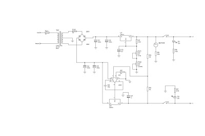
This is a bench top power supply that can be used to power circuits or devices during development work in the lab. More specifically it is an adjustable, tracking, dual rail supply which means there are two supply voltages, one positive, one negative, that are adjusted by a common potentiometer such that supply voltages are equal in magnitude. It is capable of supplying up to +/- 15V DC at up to 1A. This is sufficient for the majority of small signal electronic projects. Dual Power Suplly Circuit diagram. Click to view larger Power Supply circuit above shows the circuit layout for this project. A centre tapped transformer (TR1) is used with two 12V secondary windings with its centre tap tied to ground. This allows positive and negative voltages to be generated with respect to the central ground. Rectification follows based upon the bridge rectifier (BR1) and smoothing capacitors (C1, C2, C4 and C5). Two linear regulators are used, an LM317 on the positive side and an LM337 on the ne...

Low Cost Power Mosfet Inverter

Image
This is simple and Low-cost circuit diagram project of simple power mosfet inverter circuit. This inverter can deliver .high-voltage ac or de, with a rectifier and filter, up to several hundred volts. Low- Cost Power Mosfet Inverter Circuit Diagram: The secondary and primary of T1-a 12.6 to 440 V power transformer, respectively-are reversed; e.g., the primary becomes the secondary and the secondary becomes the primary. Transistors Q1 and Q2 can be any power FET. Note: Be sure to heat sink Q1 and Q2. Capacitors C1 and C2 are used as spike suppressors.

Power LED Driver

Image
If you want to operate power LEDS with a truly constant current which significantly prolongs the lifetime of the lamp and avoid the power loss resulting from using a constant voltage supply with a series resistor, you need a suit-able constant current source. However, the only way to achieve really good efficiency is to use a switching regulator. Altogether, this means that you need a switching regulator designed to generate a constant current instead of a constant voltage. With this in mind, the author started working on the development of a LED pocket torch with especially high efficiency. Along with using high-capacity rechargeable batteries to maximise operating life, it’s worthwhile to be able to reduce the brightness, and therefore the operating current of the LEDs, when you don’t need full power. Accordingly, the author incorporated a dimming function in the design, based on operation in PWM mode in to reduce power losses to an absolute minimum. Power LED Driver Circuit Diagram ...

15 V 1 A Regulated Power Supply

Image
Here is very Simple build power supply Electronic Circuit Project of   15-V 1-A Regulated Power Supply circuit.   The supply receives - 20 V from the rectifier/filter which is fed to the collector of the Darlington pnp pass transistor, a TIP105. The base drive to the TIP105 is supplied through resistor R5. The base of the TIP105 is driven from Vz terminal at pin 9, which is the anode of a 6.2-V zener diode that connects to the emitter of the uA723 output control transistor. 15-V 1-A Regulated Power Supply Circuit Diagram: The method of providing the positive feedback required for foldback action is shown. This technique introduces positive feedback by increased current flow through resistors R1 and R2 under short-circuit conditions. This forward biases the base-emitter junction of the 2N2907 sensing transistor, which reduces base drive to the TIP105. 

3 Level Audio Power Indicator

Image
This circuit is designed to indicate the power level output of any audio amplifier. It's simple, portable, and displays three power levels can be adjusted to any desired value. For a standard power amplifier hi-fi stereo, the output values ​​suggested are: D5 illuminates at 2W D4 illuminates at 12.5W D3 illuminates at 24.5W The above values ​​were selected for easy setup, but other options are possible. IC1A is the input buffer, feeding 3 voltage comparators and LEDs drivers by means of a variable DC voltage obtained by R5 and C4 smoothing action. In order to achieve stability of adjustment, the supply of IC1 and trimmers R6 and R7 is reduced and is subject to 5.1V by Zener diode D1.

Multiple output switching power supply circuit

Image
This power supply uses two VN400A 400 Volts  MOSFETs in a half-bridge power switch configuration. Each output consists of +5V at 20 A and 15 V at 1 A . Three-terminal regulators are used for the low-currents outputs , either 12 Volts or 15 Volts can be made available with a simple change in the transformer secondary windings. Schematic diagram below : IC TL494 switching regulator IC provides pulse-with modulation control and drive signals for the power supply , The upper MOSFET , Q7 , in the power switch stage is driven by a simple transformer drive circuit. The lower MOSFET , Q6 , since it ground referenced , is directly driven from the control IC.

LM338 Power Supply 13 8V 5A

Image
This ac to dc power supply can output 5A in continous operation and 12A peak current. This kind of dc power supplies uses a PCB so you can use two case types for IC1, TO-220 or TO-3. The regulation of this 12 volt power supply is made with TR1 ( multiturn ). IC1 must be placed on proper heatsink. LM338 Power Supply Circuit Diagram :

Low Power Audio Amplifier Circuit with IC TDA2824S

Image
This is stereo audio amplifier with based on ICTDA2824S , Minimum voltage require 3 volts and maximum voltage 17 volts . Maximum output power 2 X 2 Watt , its low power amplifier. Output impedance  4 ohm. see schematic audio below :

Power Resumption Alarm and Low Voltage Protector

Image
The circuit described here protects your electrical appliances like AC motors from damage due to low voltage at power-on. It remains standby without giving power to the load after power resumes. The load can be switched on only manually. This prevents damage to the device if it is 'on' when power resumes. unregulated power supply is derived from a 12V-0-12V, 300mA step-down transformer and rectifying diodes D2 and D3. The rectified DC is made ripple-free using capacitor C3. An audio/video indicator (piezobuzzer and LED3) is provided along with the power supply for power resumption. When power is switched on, capacitor C4 charges through the piezobuzzer and LED3, making both of them active. The piezobuzzer beeps and LED3 glows for a few seconds. When capacitor C4 is fully charged, the cathode of the LED becomes high inhibiting further flow of current through the buzzer. When the power is off, capacitor C4 discharges through resistor R9. The circuit uses IC CA3140 (IC1) as a volt...

Non Contact Power Monitor circuit

Image
Non-Contact Power Monitor Circuit diagram. Here is a simple non-contact AC power monitor for home appliances and laboratory equipment that should remain continuously switched-on. A fuse failure or power breakdown in the equipment going unnoticed may cause irreparable loss. The monitor sounds an alarm on detecting power failure to the equipment. The circuit is built around CMOS IC CD4011 utilising only a few components. NAND gates N1 and N2 of the IC are wired as an oscillator that drives a piezobuzzer directly. Resistors R2 and R3 and capacitor C2 are the oscillator components. The amplifier comprising transistors T1 and T2 disables the oscillator when mains power is available. In the standby mode, the base of T1 picks up 50Hz mains hum during the positive half cycles of AC and T1 conducts. Non-Contact Power Monitor Circuit diagram:     Non-Contact Power Monitor circuit diagram    This provides base current to T2 and it also conducts, pulling the collector to gr...

Nuclear power how it can works

Image

Philco PH32M LED LCD TV Power supply and audio output section schematic

Image
Used ICs: JRC4558, TDA7266SA, NCP1606B, LD7531, 5A500V[FET], SG3525, LM358,  Audio output SMPS [Click on the schematics to zoom]

Regulator power supply with op amp

Image
Power supply circuit has a first amplifier using op-amp is IC uA741. Op amp circuit that is used only one, but it also features an adjustable voltage, which is steered by a trimpot resistors. Rtrim will set the input to the IC input on pin 2, so that if the detainee on Rtrim which will be channeled into ic enlarges the output voltage will be small, and otherwise. After the voltage is boosted and filtered and then the voltage will be regulated and boosted again by a NPN transistor. Output voltage 0.5V - 35V Part List : Resistor R1____1K5 R2____1K trim R3____10K R4____330R R5____1K R6____47R R7____68R R8____820R R9____47K R10___22K R11___1K5 Capacitor C1____10000uF 80V Transistor Q1____2N3565 Q2____2N3565 Q3____S9013 Q4____S9013 Diode D1____1N4007 D2____1N4007 LED1_Red Led IC U1____uA741 (op-amp ic)

Class AB Power Amplifier Circuit 30w Using Power Transistor

Image
Class AB Power Amplifier Circuit Diagram 30W Class AB power amplifier circuit diagram using power transistor . Set the above amplifier up by adjust the variable resistor R1 to maximum and R12 to zero. After this set up is done, the activate / turn on the amplifier . Adjust the R1 so that the measured output offset is between 30 and 100mV. Once set, adjust the R12 slowly to achieve a quiescent current of around 120mA. Keep checking the quiescent current as the amplifier heats up as it might change due to voltage drop changes in the output devices because of the heat. The heatsinks should be 0.6K/W or less for two amplifiers . Power supply circuit for 30W class AB power amplifier: 30W Class AB Power Amplifier Circuit, 

Power Supply with tube

Image
Power supply with Z2C tubes are designed specifically to provide power supply voltage to the EL-34 tube amplifier push-pull in the previous article. Power supply with Z2C tube to tube power amplifier is made with a tube rectifier Z2C. Just as the power supply for power amplifier tube earlier, power supply also uses a filter 3 levels with kapsitor electrolyte. Circuit power supply with tube rectifier Z2C can give +210 VDC output voltage. A complete range of power supply for power amplifier tube can be seen in thethe following figure . Power Supply with tube Z2C on the rectifier tube in power supply with tube above require a supply voltage for the filaments taken from the other side of the transformer secondary. Power supply with Z2C tube is a power supply that dapt used as a substitute power supply for power amplifier tubes .

Tube Power Amplifier 35W Push Pull

Image
Tube Power Amplifier 35W Push Pull is made using a tube and eventually compiled configuration push-pull amplifier. Tube Power Amplifier 35W Push Pull tube til it using EL-34 as the amplifier end. In the power amplifier that is made with a tube at a glance looks simple because the use of active components that are not complex. It should be noted that the use of tubes in Tube Power Amplifier 35W Push Pull require a high voltage supply, therefore in the process of making and finishing must be careful of high voltage and radiation. Detailed series of Tube Power Amplifier 35W Push Pull can be seen in the following figure. Tube Power Amplifier Series 35W Push Pull Sign Components Tube Power Amplifier 35W Push Pull R1 = 470K 0.5 W R2-5 = 2K2 0.5W R3 = 150K 0.5W R4 = 220K 0.5W R6-10 = 56K 0.5W R7 = 3.9K 0.5W R8 = 220R 0.5W R9 = 1M 0.5W R11 = 39K 1W R12-23 = 180K 0.5W R13-21 = 820K 0.5W R14-22 = 5K6 0.5W R15-20 = 680K 0.5W R16-19 = 100K 0.5W R17-18 = 3K3 1W R24 = 470R 2W TR1-2 = 470R 1W Variabl...

The pair of transistors power amplifier

Image
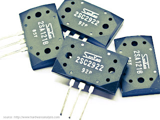
Already Know about the transistor above? transistor above is one of the transistors that are applied at the amplifier end audio amplifiers. Because the power output and good quality of this transistor is very popular with high-power amplifier makers. Transistors on no other than is 2SC2922 and 2SA1216, transistor pair is already very well known as a reliable amplifier. With a price not too expensive and not too large transistor large is also very suitable. And this transistor has its own code for its quality, its code is like 5DY, 57P, 85Y, 92P, etc.. to see datsheet transistor can be seen below. Maximum Voltage  180V maximum collector current  17A Total power output  200W To more clearly and accurately datasheet can be found here.

Stable USB Power Supply Circuit Diagram

Image
A common problem when an AC mains adapter is used to power a USB device is that the voltage does not match the nominal 5 V specified by the USB standard. The circuit shown here accepts an input voltage in the range of 4-9 V and converts it into a 6-V output voltage, which is then stabilized to a clean 5-V level by a series regulator. The combined boost/buck converter used here operates on the SEPIC principle. That principle is quite similar to the operating principle of the Cuk converter, but without the disadvantage of a negative output voltage. Circuit diagram : Stable USB Power Supply Circuit Diagram The circuit is built around a MAX668, which is intended to be used as a controller for boost converters. The difference between a SEPIC converter and a standard boost (step-up) converter is that the former type has an additional capacitor (in this case C2) and a second inductor (in this case, the secondary winding of transformer L1). If C2 is replaced by a wire bridge and the secondary...

9 Volt Power Supply Circuit Diagram Using IC 7809

Image
Description Circuit showing a 9 volt power supply . Here we have used a bridge rectifier and 7809 ic for making this circuit.Where the ic regulate the output to 9 v,1 A .This voltage every time constant.Are you interested ? Circuit diagram with Parts list.    Notes.  If a current of 300 mA or above is required, fit a proper heat sink to the IC 7809 . If 1A bridge is not available, make one using four 1N 4007 diodes.

11W Stereo or 22 W Mono Power Amp Circuits

Image
Eleven W Stereo or 22 W Mono Power Amp . Integrated AF power amps have seen great improvements in recent years offering improved power and easier use. The TDA1519C from Philips contains two power amplifiers providing 11 W per channel stereo or 22 W mono when the two channels are connected in a bridge configuration. The special in-line SIL9P package outline allows the chip to be conveniently bolted to a suitable heatsink. The TDA1519CSP is the SMD version, in this case the heat sink is mounted over, and in contact with, the top surface of the chip.  11W Stereo Amplifier Circuit Diagram The operating voltage of this device is from +6V to +17.5V. The two channels of the amplifier are different in that one channel, between pins 1 and 4, is a non-inverting amplifier, while the other between pins 9 and 6 is an inverting amplifier. It is therefore necessary in stereo operation, to wire the speakers so that one of them has its polarity reversed. Each amplifier has an input impedance of 60kΩ...